Nanoparticle Inks: Buffer Layers for Printed Electronics
Printed electronics are uniquely complex, requiring high-performance materials with outstanding functionalities that can be applied to substrates in multi-layered structures through simple and cost-efficient processing methods. The properties of these individual layers determine their interactive capabilities, which in-turn governs the functional capacities of the device macrostructure. Electronic inks for printing applications are typically comprised of nanoparticle dispersions, with multiple established arrangements for stacking electronically-active materials in high functionality thin-film arrays.
This blog post will explore the use of electronic inks as buffer layers between the electrodes of a printed electronic system.
HTL Electronic Inks for Printing
The hole transport layer (HTL) in a thin film array such as an organic photovoltaic (OPV) cell is used as a primary buffer layer between the lower or uppermost electrode and the photoactive layer. It allows the transport of holes while blocking electrons. Conversely, the electron transport layer (ETL) is used to transport electrons and block holes.
Solution-processed poly (3,4-ethylene dioxythiophene) polystyrene sulfonate (PEDOT-PSS) is a unique polymer mixture that has been used as an HTL material in normal thin film arrangements. It can provide decent device functionality but is less suited for inverted architectural systems due to the material’s acidity and long-term instability.
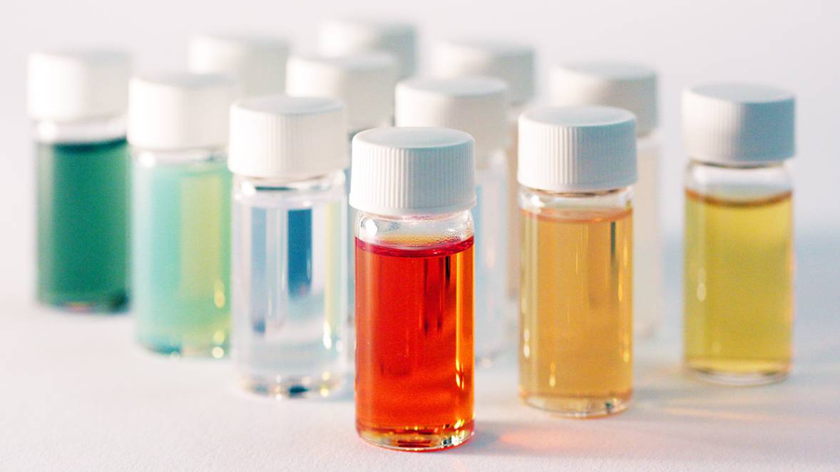
To improve the lifetime of printed electronic HTL layers without reducing their processability, Avantama has developed solutions for printing organic electronic architectural structures. High purity tungsten trioxide (WO3) in an isopropanol solvent exhibits exceptional physical stability and can be ink printed onto both hydrophilic and hydrophobic substrates to fabricate various printed electronic substrates, including OPVs and organic light-emitting diodes (OLEDs).
This HTL electronic ink can be processed through numerous coating and printing methodologies, including ink-jet printing at room temperature with an annealing time of less than 100°C.
Electron Transport Layer Electronic Inks
Inorganic nanoparticle inks such as zinc oxide (ZnO) typically exhibit improved stability over organic materials for the ETL layer but lack the required processability for cost-effective electronic printing. Sol-gel solution processing of ZnO nanoparticle inks can also damage the active layer of the thin-film array with insufficient yield due to poor electrical contact with the electrode.
Avantama has developed specialized electronic inks for printing applications comprised of aluminum-doped ZnO nanoparticles, with strict control of the aluminum content to the sub-parts per million range. This works in conjunction with WO3 HTL nanoparticle inks and can be processed using established slot-dye and ink-jet printing methods.
Benefits of Avantama Nanoparticle Ink Buffer Layers
Avantama’s nanoparticle inks are capable of full solution processing with competitively low post-treatment temperatures and outstanding material flexibility. These functional materials are proven to yield good interfacing layers that are resistant to gradual degradation
We are on the leading edge of material innovations for printed electronics, providing unique nanoparticle solutions for numerous industry requirements with short development cycles and exceptional lot-to-lot reproducibility.
If you would like any more information about using our nanoparticle inks for buffer layers in printed electronics, please do not hesitate to contact us.