avamox for Optical Sensors
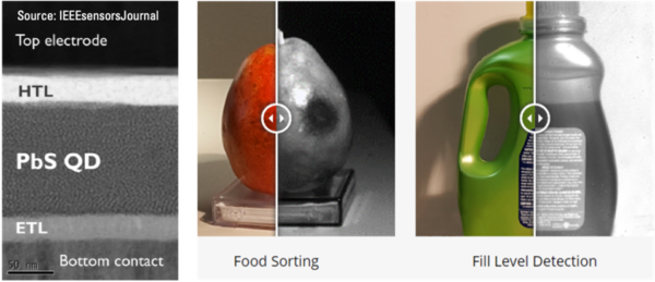
We have developed highly efficient solution processable inorganic charge transport formulations for optical sensors such as SWIR sensors or fingerprint sensors. Our formulations yield very thin and stable metal oxide layers with either hole transport (HTL) or electron transport (ETL) function.


Off-the-shelf ETL and HTL materials, customization on request
Our off-the-shelf portfolio comprises almost 30 different standard formulations suitable for both hole and electron transport functions. With a suitable solution for practically every modern printing and coating technique, Avantama can support the production of your electronic device via spin coating, ink jet printing, roll-to-roll coating, and many more.
- Various ETL/HTL compositions are available off-the-shelf
- ZnO, Al:ZnO
- SnO2; Sb:SnO2
- NiO
- WO3
- Various solvent systems for different coating/printing processes
- Nanoparticle solid loadings: 1 – 10 wt%
- Proprietary ligands for:
- High ink shelf life (12+ months)
- good charge transport
- Ink formulations tunable on customer’s specifications (e.g. solid loading, solvent system, etc.)

Advantages of Avantama ETL and HTL materials
Enabling high-volume mass production of Perovskite PV
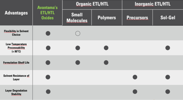
Compared to other materials in the market, Avantama avamox materials have the following advantages for the use as ETL and HTL materials:
- Solution processable
→ For e.g. roll-to-roll high-volume Perovskite PV manufacturing - Low-temperature processing (< 80°C)
→ For temperature-sensitive substrates and fast deposition/drying times - Coatable on various substrates
- High ink production reproducibility
- High ink shelf life (12+ months)
→ Key for mass production of Perovskite PV - Nanoparticle and ink production capacity equivalent to 0.2 – 2 GW Perovskite PV/year
- Customer-specific ink customization available

We also offer a tailored design and synthesis service, to assist in the development of proprietary formulations based on unique chemistries. Contact us if you would like to learn more.


