How Do OLEDs Work?
Currently dominating premium consumer displays, organic light-emitting diodes (OLEDs) are renowned for their black levels, contrast ratios, and HDR (high dynamic range) efficacy. In fact, the unique brightness capabilities of OLED panels mandated a secondary standard of certification for HDR-compatibility.
Display technologies previously had to generate a minimum peak brightness of 1,000 nits, equivalent to 1,000 candelas per square meter (cd/m2) to achieve the HDR standard. OLED televisions, by comparison, can produce vivid, HDR content with almost half that output: approximately 540 nits. This unprecedented efficiency has established OLED panels as the best dynamic range displays on the market – but how do OLED TVs actually work?
Avantama is one of the industry-leading formulators of nanoparticle solutions for printed electronics applications. In this blog post, we aim to explain how OLEDs work, answering how OLEDs emit light and why they are so readily compatible with next-generation content formats like HDR10+ and Dolby Vision.
Working Principles of OLED Devices
OLEDs are composite systems arranged in a lamellar structure; much like liquid crystal displays (LCDs), which monopolized the TV industry for years before the onset of OLED panels. The primary component in this structure is the photoemitter, and the emitter itself is arranged in a similar layered structure comprising sequentially deposited organic inks with different photoelectronic properties. These are sandwiched between an anode and a cathode, turning this photo-emissive stack into a self-contained circuit.
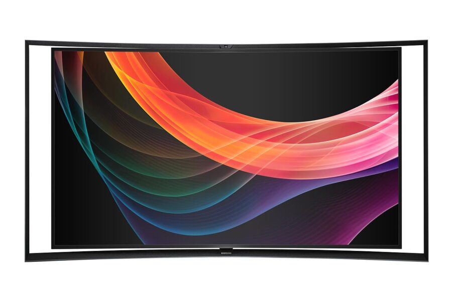
Source: Samsung Belgium
If you would like to learn more information about manufacturing OLEDs, read our previous article: How are OLEDs Made?
In the most basic structure, OLED panels comprise a bilayer photoemitter with a conductive and emissive layer. When a voltage is applied to the circuit, a current of electrons flows through the stack, resulting in the recombination of electrons and electron holes near the bilayer interface. The energy levels of the resulting excitons gradually relax, yielding a loss of energy in the form of light. The wavelength of light emitted, meanwhile, is determined by the patterning of pixels in the emissive layer. There are two primary approaches to this:
- Generate an RGB (red, blue, and green) pattern of sub-pixels for every pixel in the emitter, or;
- Generate white light in every pixel and filter it with a supplementary color filter.
The former is by far the preferred method as it produces crisper images with clear pixel-to-pixel definition. It also means that each individual pixel can be switched off dynamically, enabling true-black representation due to the lack of light bleeding over from neighboring pixels. This type of photo emitter is why OLED panels satisfy the needs of HDR10+ and Dolby Vision with just 540 nits of peak brightness.

Innovations in nanoparticle dispersions and OLED engineering have enabled developers to produce sophisticated multilayer thin film stacks comprised of finely-tailored electronic layers. A typical structure for OLED panels today might include:
- Cathode
- Electron Transport Layer (ETL)
- Blocking Layer
- Emissive Layer
- Hole Transport Layer (HTL)
- Hole Injection Layer
- Anode
Solution-Processed OLEDs from Avantama
Avantama specializes in the development of novel formulations for advanced electronics applications. We have generated an established portfolio of nanoparticle inks that are compatible with the broadest possible range of manufacturing techniques for printable charge transport materials. Fully-tailored materials are also available for specific customer requirements.
For more OLED news and information, read our article 4 Current Applications for OLED Devices
If you would like to discuss your OLED manufacturing needs and requirements, simply contact a member of the Avantama team today.
References: