Applications of Solution-Processed OLEDs
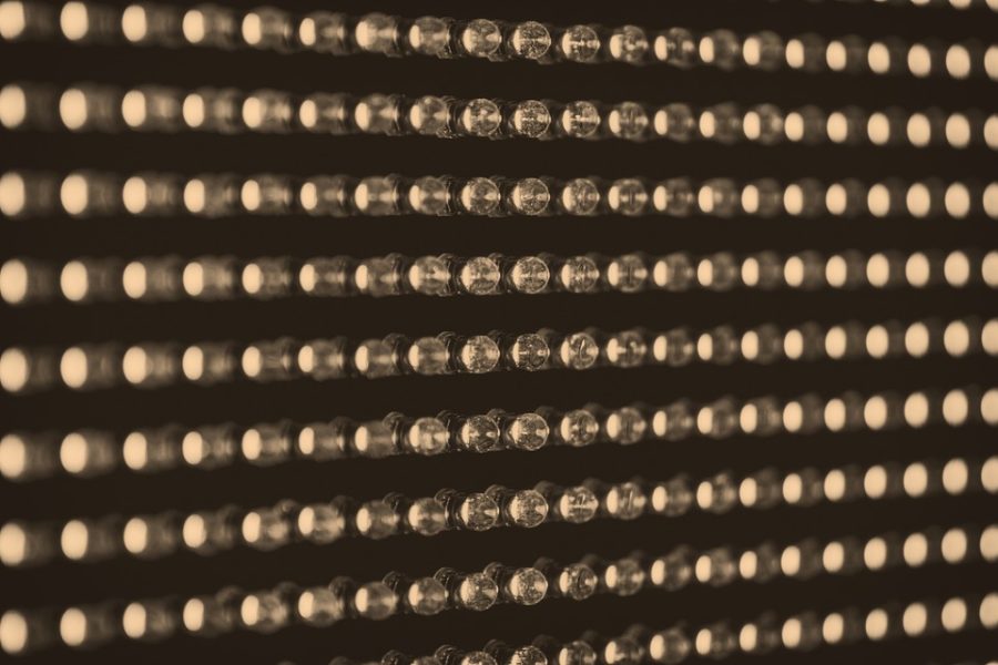
Organic light-emitting diodes (OLEDs) are solid-state devices based on thin films of semiconducting nanomaterials and electroluminescent organic molecules or polymers arranged in sequential layers. Basic OLED panels induce currents using a cathode, which introduces electrons into the emissive layer of the array. An anode removes these electrons, leaving electron holes. The result is a highly efficient photo-emissive stack.
Read More: How Do OLEDs Work?
The problem with OLED technology is the manufacturing bottleneck. Conventional production methods, like vacuum thermal evaporation (VTE), are costly and time-consuming, requiring a low-pressure vacuum chamber, finely-tuned temperature control, and vapor-phase organic materials. This also limits the panel size to relatively small dimensions compared to conventional LED-backlit panels. OLED manufacturers have been fortunate in the sense that small form factor OLED displays can readily service the smartphone and electronic wearables market. However, the cost of producing larger panels remains prohibitive.
Solution-Processed OLEDs: Primarily Prototypes
Solution-processed OLEDs are an increasingly attractive alternative to VTE-produced panels for mid- to large-panel displays. Using a choice of conventional printing techniques (inkjet, spin coating, roll-to-roll, etc.), functional organic layers can be uniformly deposited onto substrates of much larger areas. Obstacles still exist to industrial-scale solution-processed OLED manufacturing, however. For example, ink-jet printing struggles to meet the same high-density batch manufacturing scales as VTE, where numerous – albeit small – OLED panels can be developed simultaneously. Consequently, VTE-OLEDs are best suited for smartphones, watches, and virtual reality headsets while solution-processed OLEDs are primarily intended for OLED lighting or the home display market.
Although increasingly accessible to display manufacturers, the solution-processing of OLEDs is still uncommon. This is primarily because the operational lifetime of solution-processed OLED panels is yet to reach the same level as thermally evaporated devices. Currently, most solution-processed OLEDs are prototypical, such as Chinese manufacturer TCL’s H-QLED; a hybrid, high-end display comprised of an ink-jet printed OLED back panel and layered red-green quantum dots (QDs). Using a blue-light OLED as a back panel for red and green QD emissive layers is theoretically one of the most energy-efficient television designs currently envisaged.
Further development is required before solution-processing becomes the primary method of OLED panel manufacturing, but the functional materials already exist. Many manufacturers believe that solution-processed OLEDs are on the verge of realization at scale, with applications varying from mid-sized consumer displays to energy-efficient lighting.
Solution-Processed OLEDs with Avantama
Avantama is one of the world-leading suppliers of nanoparticle inks for printed electronics applications. We have pioneered a series of off-the-shelf functional materials alongside our proprietary formulation service, through which you can develop bespoke nanoparticle formulations for your manufacturing needs.
If you would like more information about producing solution-processed OLEDs with Avantama inks, simply contact a member of the team today.